


Integrated Photonics Testing
Summary
 What are photonic integrated circuits (PICs)?
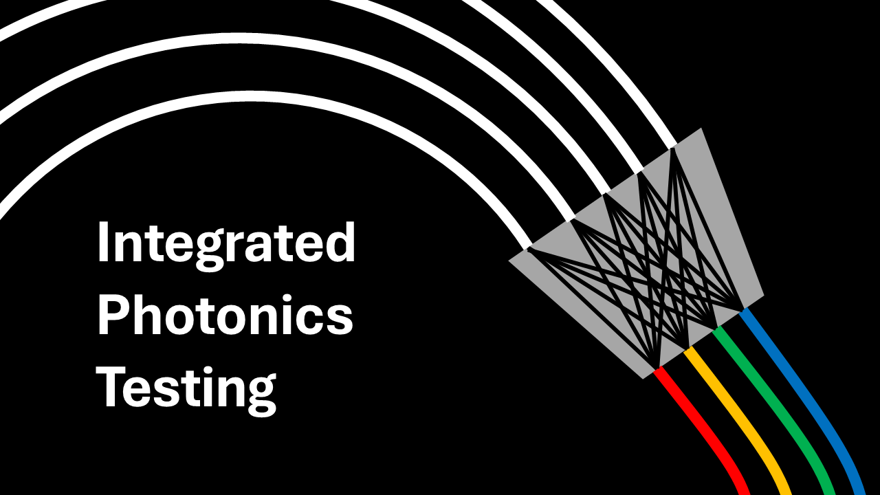
Much like integrated electrical cicuits, PICs consist of multiple photonic devices on a single substrate. Instead of electrons in a traditional circuit, photons travel between the devices on the PIC which manipulate or detect light. Since PICs are compace, they reduce the size, weight, and power (SWaP) of an optical system which makes them an ideal solution for optical applications that require a small footprint.
This project, funded by the Economic Development Administration (EDA) through the Headwaters Tech Hub (HTH) and the Montana Photonics & Quantum Alliance (MPQA) has two main parts:
- Develop infrastructure, including user facilities and capabilities to test PICs
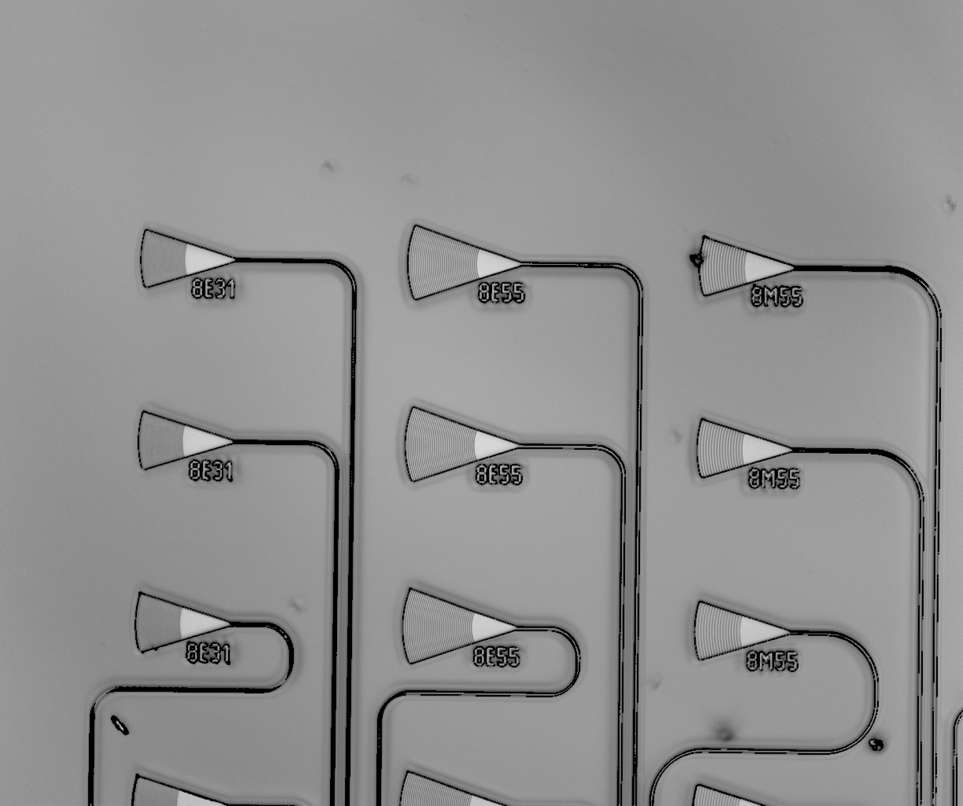
- Develop devices with internal and external customers
Capabilities
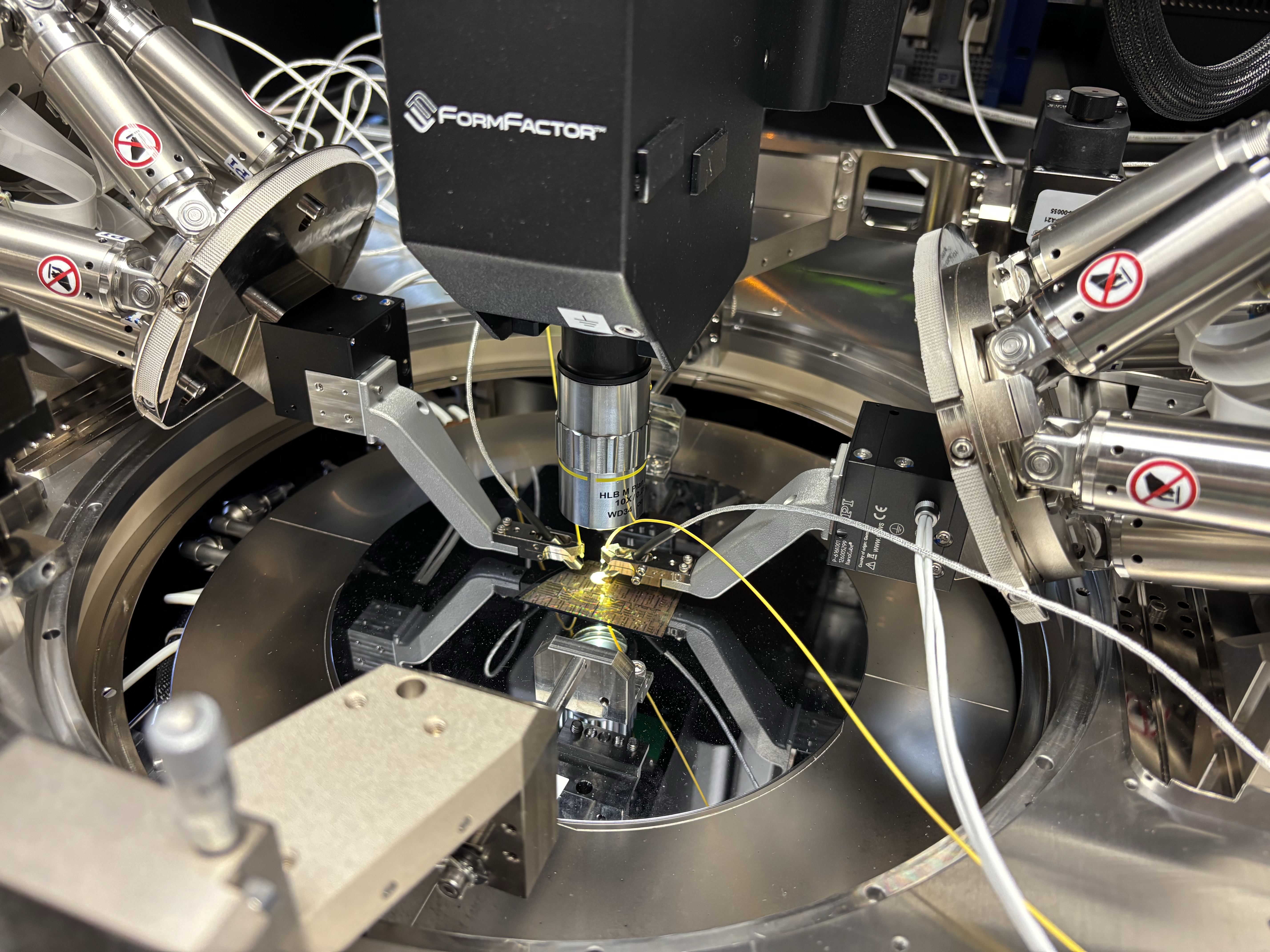
At Spectrum Lab, we are developing a PIC testing lab, including automated 300 mm wafter test station and a manual die test station. These capabilities will allow MSU researchers and the wider optics and photonics ecosystem in the Gallatin Valley to rapidly design and test PICs locally, ensuring theat Bozeman stays competitive in the photonics industry.
Testing facilities include:
- 300 mm wafer automated wafer probe station (for multiple die measurements)
- Manual die probe station
Personnel
Dr. Corey Pearson (coreypearson@montana.edu)
Dr. Dennis Dempsey (dennis.dempsey@montana.edu)
Graduate Researcher
Michael Menuey, MS, Electrical Engineering
Undergraduate Researchers
Grace Brockie, Undergraduate, Electrical Engineering
Zachary Rice, Undergraduate, Physics